Buck-Boost Converters
A Buck-Boost converter is a type of switched mode power supply that combines the principles of the Buck Converter and the Boost converter in a single circuit. Like other SMPS designs, it provides a regulated DC output voltage from either an AC or a DC input.
The Buck converter described in Power Supplies Module 3.1 produces a DC output in a range from 0V to just less than the input voltage. The boost converter will produce an output voltage ranging from the same voltage as the input, to a level much higher than the input.
There are many applications however, such as battery-powered systems, where the input voltage can vary widely, starting at full charge and gradually decreasing as the battery charge is used up. At full charge, where the battery voltage may be higher than actually needed by the circuit being powered, a buck regulator would be ideal to keep the supply voltage steady. However as the charge diminishes the input voltage falls below the level required by the circuit, and either the battery must be discarded or re-charged; at this point the ideal alternative would be the boost regulator described in Power Supplies Module 3.2.
By combining these two regulator designs it is possible to have a regulator circuit that can cope with a wide range of input voltages both higher or lower than that needed by the circuit. Fortunately both buck and boost converters use very similar components; they just need to be re-arranged, depending on the level of the input voltage.
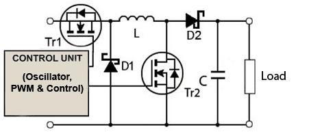
Fig. 3.3.1 Buck and Boost Converters Combined
In Fig. 3.3.1 the common components of the buck and boost circuits are combined. A control unit is added, which senses the level of input voltage, then selects the appropriate circuit action. (Note that in the examples in this section the transistors are shown as MOSFETs, commonly used in high frequency power converters, and the diodes shown as Schottky types. These diodes have a low forward junction voltage when conducting, and are able to switch at high speeds).
Operation as a Buck Converter
The basic operation of the buck boost converter is illustrated in Figs. 3.3.2 to 3.3.5
Fig. 3.3.2 shows the circuit operating as a Buck Converter. In this mode Tr2 is turned off, and Tr1 is switched on and off by a high frequency square wave from the control unit. When the gate of Tr1 is high, current flows though L, charging its magnetic field, charging C and supplying the load. The Schottky diode D1 is turned off due to the positive voltage on its cathode.
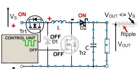
Fig. 3.3.2 Operation as a Buck Converter During Tr1 ‘on’ Period
Fig 3.3.3 shows the current flow during the buck operation of the circuit when the control unit switches Tr1 off. The initial source of current is now the inductor L. Its magnetic field is collapsing, the back e.m.f. generated by the collapsing field reverses the polarity of the voltage across L, which turns on D1 and current flows through D2 and the load.
As the current due to the discharge of L decreases, the charge accumulated in C during the on period of Tr1 now also adds to the current flowing through the load, keeping VOUT reasonably constant during the off period. This helps keep the ripple amplitude to a minimum and VOUT close to the value of VS.
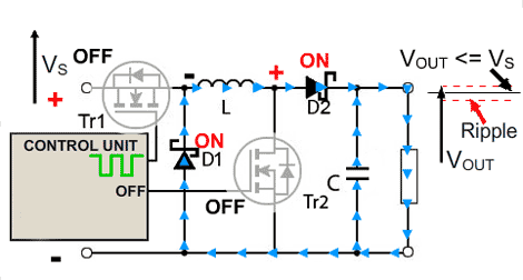
Fig. 3.3.3 Operation as a Buck Converter During Tr1 ‘off’ Period
Operation as a Boost Converter
In Boost Converter mode, Tr1 is turned on continually and the high frequency square wave applied to Tr2 gate. During the on periods when Tr2 is conducting, the input current flows through the inductor L and via Tr2, directly back to the supply negative terminal charging up the magnetic field around L. Whilst this is happening D2 cannot conduct as its anode is being held at ground potential by the heavily conducting Tr2. For the duration of the on period, the load is being supplied entirely by the charge on the capacitor C, built up on previous oscillator cycles. The gradual discharge of C during the on period (and its subsequent recharging) accounts for the amount of high frequency ripple on the output voltage, which is at a potential of approximately VS+ VL.
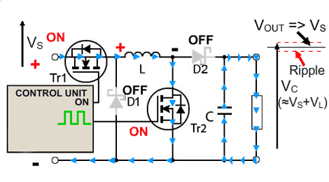
Fig. 3.3.4 Operation as a Boost Converter During Tr2 ‘on’ Period
The Off Period
At the start of the off period of Tr2, L is charged and C is partially discharged. The inductor L now generates a back e.m.f. and its value that depends on the rate of change of current as Tr2 switches of and on the amount of inductance the coil possesses; therefore the back e.m.f can be any voltage over a wide range, depending on the design of the circuit. Notice particularly that the polarity of the voltage across L has now reversed, and so adds to the input voltage VS giving an output voltage that is at least equal to or greater than the input voltage. D2 is now forward biased and so the circuit current supplies the load current, and at the same time re-charges the capacitor to VS + VLready for the next on period of Tr2
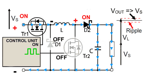
Fig. 3.3.5 Operation as a Boost Converter During Tr2 ‘off’ Period
Circuit Variations
There are a number of variations of this basic Buck-Boost circuit, some designs working at lower frequencies or at high voltages may use bipolar transistors instead of MOSFETs; at low frequencies the higher speed switching of MOSFETs is less of an advantage. Also, in high voltage designs, silicon diodes may be used in preference to Schottky types due to the silicon diode’s higher reverse voltage capabilities. Another variation is to use synchronous switching where, instead of using diodes that simply respond to the voltage polarity across them, four synchronised (by the control unit) MOSFETs do all the switching.
The control unit may also carry out over current and over voltage protection, as well as the normal oscillator and pulse width modulation functions to regulate the output voltage.
Another commonly used facility is ‘pulse skipping’ where the control unit prevents charging on one or more oscillator pulses when it senses that the load current is low. This reduces the overall current drawn from the (typically battery) supply, prolonging battery life.
Buck-Boost Converter I.Cs. are commonly used to carry out the control unit functions. These range from very low power, high efficiency I.Cs. for portable devices such as mobile phones and automotive applications, such as the TPS63000 series from Texas Instruments, and the LTC3789from Linear Technology, to large industrial high power DC-DC converters providing many kilowatts of output power.

Great! So useful
ReplyDeleteWe desire to see the feedback from the output!