
Boost Converter
Switched mode supplies can be used for many purposes including DC to DC converters. Often, although a DC supply, such as a battery may be available, its available voltage is not suitable for the system being supplied. For example, the motors used in driving electric automobiles require much higher voltages, in the region of 500V, than could be supplied by a battery alone. Even if banks of batteries were used, the extra weight and space taken up would be too great to be practical. The answer to this problem is to use fewer batteries and to boost the available DC voltage to the required level by using a boost converter. Another problem with batteries, large or small, is that their output voltage varies as the available charge is used up, and at some point the battery voltage becomes too low to power the circuit being supplied. However, if this low output level can be boosted back up to a useful level again, by using a boost converter, the life of the battery can be extended.
The DC input to a boost converter can be from many sources as well as batteries, such as rectified AC from the mains supply, or DC from solar panels, fuel cells, dynamos and DC generators. The boost converter is different to the Buck Converter in that it’s output voltage is equal to, or greater than its input voltage. However it is important to remember that, as power (P) = voltage (V) x current (I), if the output voltage is increased, the available output current must decrease.
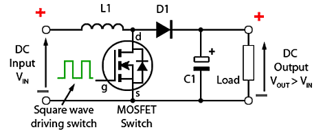
Fig. 3.2.1 Basic Boost Converter Circuit
Fig. 3.2.1 illustrates the basic circuit of a Boost converter. However, in this example the switching transistor is a power MOSFET, both Bipolar power transistors and MOSFETs are used in power switching, the choice being determined by the current, voltage, switching speed and cost considerations. The rest of the components are the same as those used in the buck converter illustrated in Fig. 3.1.2, except that their positions have been rearranged.
Boost converter Operation
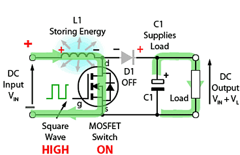
Fig 3.2.2 illustrates the circuit action during the initial high period of the high frequency square wave applied to the MOSFET gate at start up. During this time MOSFET conducts, placing a short circuit from the right hand side of L1 to the negative input supply terminal. Therefore a current flows between the positive and negative supply terminals through L1, which stores energy in its magnetic field. There is virtually no current flowing in the remainder of the circuit as the combination of D1, C1 and the load represent a much higher impedance than the path directly through the heavily conducting MOSFET

Fig. 3.2.2 Boost Converter Operation at Switch On
Fig. 3.2.3 shows the current path during the low period of the switching square wave cycle. As the MOSFET is rapidly turned off the sudden drop in current causes L1 to produce a back e.m.f. in the opposite polarity to the voltage across L1 during the on period, to keep current flowing. This results in two voltages, the supply voltage VIN and the back e.m.f.(VL) across L1 in series with each other.
This higher voltage (VIN +VL), now that there is no current path through the MOSFET, forward biases D1. The resulting current through D1 charges up C1 to VIN +VL minus the small forward voltage drop across D1, and also supplies the load
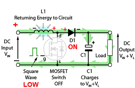
Fig.3.2.4 shows the circuit action during MOSFET on periods after the initial start up. Each time the MOSFET conducts, the cathode of D1 is more positive than its anode, due to the charge on C1. D1 is therefore turned off so the output of the circuit is isolated from the input, however the load continues to be supplied with VIN +VL from the charge on C1. Although the charge C1 drains away through the load during this period, C1 is recharged each time the MOSFET switches off, so maintaining an almost steady output voltage across the load.
The theoretical DC output voltage is determined by the input voltage (VIN) divided by 1 minus the duty cycle (D) of the switching waveform, which will be some figure between 0 and 1 (corresponding to 0 to 100%) and therefore can be determined using the following formula:
Example:
If the switching square wave has a period of 10µs, the input voltage is 9V and the ON is half of the periodic time, i.e. 5µs, then the output voltage will be:
VOUT = 9/(1- 0.5) = 9/0.5 = 18V (minus output diode voltage drop)
Because the output voltage is dependent on the duty cycle, it is important that this is accurately controlled. For example if the duty cycle increased from 0.5 to 0.99 the output voltage produced would be:
VOUT = 9/(1- 0.99) = 9/0.01 = 900V
Before this level of output voltage was reached however, there would of course be some serious damage (and smoke) caused, so in practice, unless the circuit is specifically designed for very high voltages, the changes in duty cycle are kept much lower than indicated in this example.
No comments:
Post a Comment