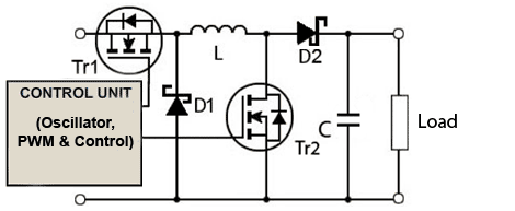
Wednesday 19 August 2015

Push-Pull Switched Mode Power Supplies

The Push Pull SMPS

SMPS-push-pull-Block.gif

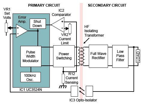
Fig. 3.4.1 Push Pull SMPS Block Diagram

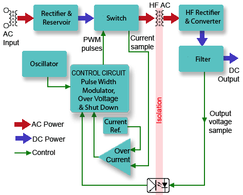
Fig. 3.4.1 shows a block diagram of a switched mode power supply designed around a UC3524 Advanced Regulating Pulse Width Modulator byTexas Instruments.
The circuit is a DC to DC converter using a DC input voltage of 15V to 30V and produces a regulated 5V output at a current up to about 250mA. The circuit uses push pull power switching driving a high frequency transformer, which fully isolates the output circuit from the input. The output is short circuit protected, and the output voltage can be manually adjusted. Maximum current can be also manually set using adjustable current limiting.

Primary Circuit.

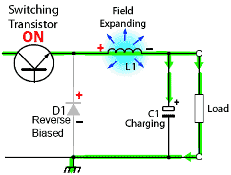
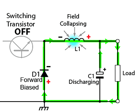
A 100kHz oscillator within IC1 (UC3524) generates pulses, which are processed by the pulse width modulator (within IC1)used to drive the power switching transistors. The width of the processed drive pulses controls the length of time for which the power switching transistors conduct, and therefore the amount of power delivered to the transformer.
The pulse width and therefore the output voltage is controlled by the error amplifier in IC1. This measures the difference between a sample of the output voltage, fedback via the opto-isolator, and a reference voltage set by Vr1. When these two voltages are equal, the circuit output voltage is correct. If there is a difference, the width of the pulses produced by the pulse width modulator is increased or decreased to correct the error.
Over current protection is provided to ensure that the supply is shut down in the event of too high a current demand at the output. The output terminals can even be shorted together without damaging the supply.
Each pulse of current in the power switching transistors produces a voltage pulse across the sensing resistor R12. The amplitude of these pulses is proportional to the current being delivered to the transformer by the switching circuit. If the peak value of any of these pulses exceeds the DC voltage set by Vr2 (Current limit) then the output from IC2 will cause pulse width modulator input to reduce the width of the pulse being produced by the modulator at that time, momentarily reducing the output voltage. If the over current condition disappears, the output voltage will be restored to its normal level, but if the load current remains high, the current limiter will continue to reduce the pulse width, dependent on the amount of over current, even down to zero in the case of a short circuit output.

The Secondary Circuit

The push pull switching transistors create an AC waveform across the transformer primary winding, and the secondary winding feeds a conventional full wave rectifier and LC low pass filter to supply the load with a stable 5V at the output terminals. Negative feedback to the voltage regulating circuit in IC1 is via the opto-isolator (IC3). The higher the output voltage, the brighter the glow from an LED sealed within the secondary side, and the larger the DC output voltage derived from pin 4 of IC3 in the primary side of the device. This voltage is used as a sample at the inverting input of the error amplifier in IC1 where it is compared with a voltage from the ‘set voltage’ control VR1, to control the pulse width modulator.

Circuit Description

The full schematic diagram for the circuit is shown in Fig. 3.4.2.
smps-push-pull-cct-02.gif

Fig. 3.4.2 Circuit diagram of a push-pull SMPS using the Texas Instruments UC3524 I.C.

UC3524N.gif

Fig. 3.4.3 The UC3524N (part detail)


The oscillator within IC1 produces narrow 100kHz (approx) pulses that are used as clock pulses for the Switch Logic within IC1. The timing components for the oscillator are R3 and C2. The ramp waveform produced as C2 charges is also used as an input to the inverting input of the comparator in IC1.
The pulse width modulator comprises the comparator within IC1 and the switching logic, which consists of a bistable and two three input NOR gates. The outputs of this block supply variable width pulses to the two transistors Qa and Qb.
The error amplifier compares a stable reference voltage on pin 1 (set by Vr1 supplied from an internally regulated 5V from pin 16) with a sample of the load voltage developed across the opto-isolator emitter resistor, R11. The resulting error voltage is used as the non-inverting input to the PWM comparator.
The facilities of the UC3524 that are used in this circuit are shown in more detail in Fig. 3.4.3 (Note: Some unused facilities of the UC3524 have been omitted for clarity, for more information see the Texas Instruments UC3524 data sheet).

Pulse Width Modulator

UC3524N-waveforms.gif

Fig. 3.4.4 UC3524N and Transformer Primary Waveforms

The action of the pulse width modulator, described by the waveforms shown in Fig. 3.4 4 is as follows:
Clock pulses (CK) from the oscillator are fed to the Bi-stable (flip-flop), which produces a square wave with a 1:1 mark/space ratio and a frequency of 50kHz, (half that of the oscillator) at its Q output, and an inverted version of this wave at its Q output.
Output Q provides an input to NOR gate a, and output Q (the opposite of Q) provides an input to NOR gates b. The logic rule for a NOR gate is that its output will be high, only when all its three inputs are low. Notice that the Q and Q signals go low at the start of alternate clock pulse low states. The clock signal also provides an input to both NOR gates.
The third input to each of the NOR gates is provided by the comparator output, which is a series of variable width low state pulses, produced by comparing the DC error voltage from the error amplifier in IC1 with the ramp produced by the oscillator timing capacitor C2.
As each NOR gate output goes high, only when all of its three input signals are low, alternate high state pulses, whose width depends on the value of the error voltage, are fed to the bases of the internal transistors Qa and Qb. The lower the value of the error voltage (due to a higher value of "sample" voltage at pin 1) the narrower the pulses produced. These narrower pulses, when used to turn on the power switching transistors TR3 and Tr4, will lead to a reduction in power in the transformer and a reduction in load voltage.

Power Switching Circuits

speed-up.gif

Fig. 3.4.5 Speeding up the Power Switch Turn Off

The internal drive transistors Qa and Qb each produces a series of pulses at its collector, and an a series of anti-phase pulses at its emitter. The emitter signals a and b drive the power switching transistors Tr3 and Tr4 respectively, and the collector signals drive the speed up circuits Tr1/Tr2.
The reason for including the speed up circuits is to overcome the delay that would normally happen because while the power switching transistors Tr3 andTr4 are conducting, their base/emitter junction (which naturally forms a small capacitor due to the depletion layer between the base and emitter layers in the transistor) is charged up, and must be discharged before the transistor will fully turn off.
The power transistor junctions are rapidly discharged by momentarily turning on Tr1 or Tr2 using a differentiated pulse generated from the rising edge of the waveform from the collector of Qa or Qb in IC1, which of course happens at exactly the same instant as Tr3 or Tr4 is turning off, as illustrated in Fig 3.4.5.
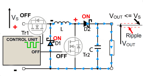
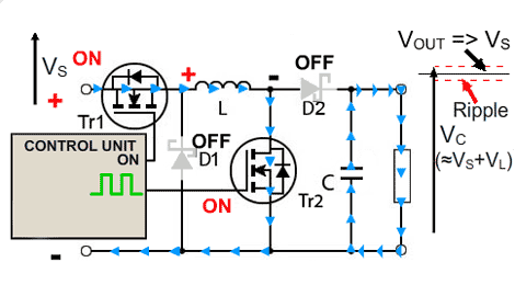
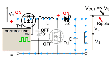
Because the transformer primary centre tap is connected to the main (+VIN) supply, it will always be at the supply potential. The collector voltages of Tr3 and Tr4 will also be at +VIN during the periods when both transistors are turned off.
During the ‘on’ pulse of Tr3, its collector will be at approximately 0V, and due to the centre tapping of the transformer primary winding the bottom half of the primary will be in anti-phase to the top half, so the collector of Tr4 will be positive at twice the value of +VIN for the period of the Tr3 ‘on’ pulse. This situation is reversed during the ‘on’ pulse of Tr4. This action produces a stepped type of waveform with an amplitude of +VIN x 2 across the transformer primary as shown in Fig 3.4.4.

The Secondary Circuit

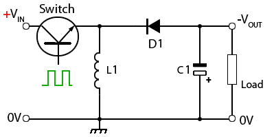
The resulting secondary voltage is rectified by D1 and D2, and smoothed by the low pass filter L1/C10 before being supplied to the load. A sample of the load voltage is fed back to the LED within opto-isolator IC3 via the LED current limiting resistor R13.
smps-transformer.jpg

Fig. 3.4.6 Typical High Frequency Multi-Secondary Transformer

Because of the push pull design used by this circuit, it is a simple matter to arrange for such a circuit to have multiple outputs. Different (higher or lower) voltages can be obtained by using a transformer similar to the one illustrated in Fig. 3.4.6, which has multiple secondary windings with appropriate turns ratios.
The total current supplied to the multiple outputs however, must not exceed the maximum current rating of the SMPS. Each supply line will have its own rectifier and filter system, and may also include some extra point of load regulation. A voltage sample will normally be taken from only one of the outputs to provide feedback to the pulse width modulator however, as controlling the power applied to the transformer primary will control all the voltage outputs.

Current limiting

Current limiting, which is capable of completely shutting down the circuit under extreme overload conditions is provided by the action of IC2 and the shut down transistor between pins 9 and 10 within IC1.
Pin 3 of IC2 is provided with a stable reference voltage derived from the shunt voltage regulator R7/ZD1 via the current limit control Vr2. The non-inverting input of IC2 is connected to a low resistance current sensing resistor R12 in the emitter lead common to both switching transistors Tr3/Tr4.
Every time either transistor conducts, the resulting large emitter current produces a voltage pulse across R12. The peak voltage of this pulse will be proportional to the emitter current flowing in Tr3/Tr4 and therefore, also to the output current.
If the peak voltage of any of these pulses applied to the non-inverting input of IC2 exceeds the stabilised DC voltage at the inverting input, a positive pulse will be produced at the output, and therefore at the base of Qc within IC1. This will cause the collector voltage of this transistor to fall, also reducing the error amplifier output that is controlling the pulse width modulator. This action has the effect of reducing the width of the pulse presently being produced, thus instantly reducing output voltage. If the current overload disappears, the pulse width modulator will return to normal operation. If not, subsequent pulses will be further reduced until the output voltage falls (if necessary) to zero.
The action of the current limit circuit is not absolutely instant however, due to the presence of C4 on the shut down compensation pin (9) of IC1. This capacitor tends to integrate the voltage changes on the collector of the shut down transistor so that very rapid (cycle by cycle) variations of the output voltage during current limiter action are avoided.

Buck-Boost Converters

Buck-Boost Converters

A Buck-Boost converter is a type of switched mode power supply that combines the principles of the Buck Converter and the Boost converter in a single circuit. Like other SMPS designs, it provides a regulated DC output voltage from either an AC or a DC input.
The Buck converter described in Power Supplies Module 3.1 produces a DC output in a range from 0V to just less than the input voltage. The boost converter will produce an output voltage ranging from the same voltage as the input, to a level much higher than the input.
There are many applications however, such as battery-powered systems, where the input voltage can vary widely, starting at full charge and gradually decreasing as the battery charge is used up. At full charge, where the battery voltage may be higher than actually needed by the circuit being powered, a buck regulator would be ideal to keep the supply voltage steady. However as the charge diminishes the input voltage falls below the level required by the circuit, and either the battery must be discarded or re-charged; at this point the ideal alternative would be the boost regulator described in Power Supplies Module 3.2.
By combining these two regulator designs it is possible to have a regulator circuit that can cope with a wide range of input voltages both higher or lower than that needed by the circuit. Fortunately both buck and boost converters use very similar components; they just need to be re-arranged, depending on the level of the input voltage.
buck-boost01.gif

Fig. 3.3.1 Buck and Boost Converters Combined

In Fig. 3.3.1 the common components of the buck and boost circuits are combined. A control unit is added, which senses the level of input voltage, then selects the appropriate circuit action. (Note that in the examples in this section the transistors are shown as MOSFETs, commonly used in high frequency power converters, and the diodes shown as Schottky types. These diodes have a low forward junction voltage when conducting, and are able to switch at high speeds).

Operation as a Buck Converter


The basic operation of the buck boost converter is illustrated in Figs. 3.3.2 to 3.3.5
Fig. 3.3.2 shows the circuit operating as a Buck Converter. In this mode Tr2 is turned off, and Tr1 is switched on and off by a high frequency square wave from the control unit. When the gate of Tr1 is high, current flows though L, charging its magnetic field, charging C and supplying the load. The Schottky diode D1 is turned off due to the positive voltage on its cathode.
buck-boost02.gif

Fig. 3.3.2 Operation as a Buck Converter During Tr1 ‘on’ Period


Fig 3.3.3 shows the current flow during the buck operation of the circuit when the control unit switches Tr1 off. The initial source of current is now the inductor L. Its magnetic field is collapsing, the back e.m.f. generated by the collapsing field reverses the polarity of the voltage across L, which turns on D1 and current flows through D2 and the load.
As the current due to the discharge of L decreases, the charge accumulated in C during the on period of Tr1 now also adds to the current flowing through the load, keeping VOUT reasonably constant during the off period. This helps keep the ripple amplitude to a minimum and VOUT close to the value of VS.
buck-boost03.gif

Fig. 3.3.3 Operation as a Buck Converter During Tr1 ‘off’ Period

Operation as a Boost Converter

In Boost Converter mode, Tr1 is turned on continually and the high frequency square wave applied to Tr2 gate. During the on periods when Tr2 is conducting, the input current flows through the inductor L and via Tr2, directly back to the supply negative terminal charging up the magnetic field around L. Whilst this is happening D2 cannot conduct as its anode is being held at ground potential by the heavily conducting Tr2. For the duration of the on period, the load is being supplied entirely by the charge on the capacitor C, built up on previous oscillator cycles. The gradual discharge of C during the on period (and its subsequent recharging) accounts for the amount of high frequency ripple on the output voltage, which is at a potential of approximately VS+ VL.
buck-boost04.gif

Fig. 3.3.4 Operation as a Boost Converter During Tr2 ‘on’ Period

The Off Period

At the start of the off period of Tr2, L is charged and C is partially discharged. The inductor L now generates a back e.m.f. and its value that depends on the rate of change of current as Tr2 switches of and on the amount of inductance the coil possesses; therefore the back e.m.f can be any voltage over a wide range, depending on the design of the circuit. Notice particularly that the polarity of the voltage across L has now reversed, and so adds to the input voltage VS giving an output voltage that is at least equal to or greater than the input voltage. D2 is now forward biased and so the circuit current supplies the load current, and at the same time re-charges the capacitor to VS + VLready for the next on period of Tr2
buck-boost05.gif

Fig. 3.3.5 Operation as a Boost Converter During Tr2 ‘off’ Period

Circuit Variations

There are a number of variations of this basic Buck-Boost circuit, some designs working at lower frequencies or at high voltages may use bipolar transistors instead of MOSFETs; at low frequencies the higher speed switching of MOSFETs is less of an advantage. Also, in high voltage designs, silicon diodes may be used in preference to Schottky types due to the silicon diode’s higher reverse voltage capabilities. Another variation is to use synchronous switching where, instead of using diodes that simply respond to the voltage polarity across them, four synchronised (by the control unit) MOSFETs do all the switching.
The control unit may also carry out over current and over voltage protection, as well as the normal oscillator and pulse width modulation functions to regulate the output voltage.
Another commonly used facility is ‘pulse skipping’ where the control unit prevents charging on one or more oscillator pulses when it senses that the load current is low. This reduces the overall current drawn from the (typically battery) supply, prolonging battery life.
Buck-Boost Converter I.Cs. are commonly used to carry out the control unit functions. These range from very low power, high efficiency I.Cs. for portable devices such as mobile phones and automotive applications, such as the TPS63000 series from Texas Instruments, and the LTC3789from Linear Technology, to large industrial high power DC-DC converters providing many kilowatts of output power.

Boost Converters

Boost Converter

Switched mode supplies can be used for many purposes including DC to DC converters. Often, although a DC supply, such as a battery may be available, its available voltage is not suitable for the system being supplied. For example, the motors used in driving electric automobiles require much higher voltages, in the region of 500V, than could be supplied by a battery alone. Even if banks of batteries were used, the extra weight and space taken up would be too great to be practical. The answer to this problem is to use fewer batteries and to boost the available DC voltage to the required level by using a boost converter. Another problem with batteries, large or small, is that their output voltage varies as the available charge is used up, and at some point the battery voltage becomes too low to power the circuit being supplied. However, if this low output level can be boosted back up to a useful level again, by using a boost converter, the life of the battery can be extended.
The DC input to a boost converter can be from many sources as well as batteries, such as rectified AC from the mains supply, or DC from solar panels, fuel cells, dynamos and DC generators. The boost converter is different to the Buck Converter in that it’s output voltage is equal to, or greater than its input voltage. However it is important to remember that, as power (P) = voltage (V) x current (I), if the output voltage is increased, the available output current must decrease.
boost-converter-basic-cct.gif

Fig. 3.2.1 Basic Boost Converter Circuit

Fig. 3.2.1 illustrates the basic circuit of a Boost converter. However, in this example the switching transistor is a power MOSFET, both Bipolar power transistors and MOSFETs are used in power switching, the choice being determined by the current, voltage, switching speed and cost considerations. The rest of the components are the same as those used in the buck converter illustrated in Fig. 3.1.2, except that their positions have been rearranged.

Boost converter Operation


Fig 3.2.2 illustrates the circuit action during the initial high period of the high frequency square wave applied to the MOSFET gate at start up. During this time MOSFET conducts, placing a short circuit from the right hand side of L1 to the negative input supply terminal. Therefore a current flows between the positive and negative supply terminals through L1, which stores energy in its magnetic field. There is virtually no current flowing in the remainder of the circuit as the combination of D1, C1 and the load represent a much higher impedance than the path directly through the heavily conducting MOSFET
boost-converter-cct01.gif

Fig. 3.2.2 Boost Converter Operation at Switch On

Fig. 3.2.3 shows the current path during the low period of the switching square wave cycle. As the MOSFET is rapidly turned off the sudden drop in current causes L1 to produce a back e.m.f. in the opposite polarity to the voltage across L1 during the on period, to keep current flowing. This results in two voltages, the supply voltage VIN and the back e.m.f.(VL) across L1 in series with each other.
This higher voltage (VIN +VL), now that there is no current path through the MOSFET, forward biases D1. The resulting current through D1 charges up C1 to VIN +VL minus the small forward voltage drop across D1, and also supplies the load
boost-converter-cct02.gif
Fig.3.2.4 shows the circuit action during MOSFET on periods after the initial start up. Each time the MOSFET conducts, the cathode of D1 is more positive than its anode, due to the charge on C1. D1 is therefore turned off so the output of the circuit is isolated from the input, however the load continues to be supplied with VIN +VL from the charge on C1. Although the charge C1 drains away through the load during this period, C1 is recharged each time the MOSFET switches off, so maintaining an almost steady output voltage across the load.
The theoretical DC output voltage is determined by the input voltage (VIN) divided by 1 minus the duty cycle (D) of the switching waveform, which will be some figure between 0 and 1 (corresponding to 0 to 100%) and therefore can be determined using the following formula:
boost-converter-cct03.gif

Example:

If the switching square wave has a period of 10µs, the input voltage is 9V and the ON is half of the periodic time, i.e. 5µs, then the output voltage will be:
VOUT = 9/(1- 0.5) = 9/0.5 = 18V (minus output diode voltage drop)
Because the output voltage is dependent on the duty cycle, it is important that this is accurately controlled. For example if the duty cycle increased from 0.5 to 0.99 the output voltage produced would be:
VOUT = 9/(1- 0.99) = 9/0.01 = 900V
Before this level of output voltage was reached however, there would of course be some serious damage (and smoke) caused, so in practice, unless the circuit is specifically designed for very high voltages, the changes in duty cycle are kept much lower than indicated in this example.

Buck Converters

The Buck Converter

SMPS-basic-2.gif

Fig. 3.1.1 The Buck Converter

The Buck Converter is used in SMPS circuits where the DC output voltage needs to be lower than the DC input voltage. The DC input can be derived from rectified AC or from any DC supply. It is useful where electrical isolation is not needed between the switching circuit and the output, but where the input is from a rectified AC source, isolation between the AC source and the rectifier could be provided by a mains isolating transformer.
The switching transistor between the input and output of the Buck Converter continually switches on and off at high frequency. To maintain a continuous output, the circuit uses the energy stored in the inductor L, during the on periods of the switching transistor, to continue supplying the load during the off periods. The circuit operation depends on what is sometimes also called a Flywheel Circuit. This is because the circuit acts rather like a mechanical flywheel that, given regularly spaced pulses of energy keeps spinning smoothly (outputting energy) at a steady rate.

AC or DC Input

The buck converter is a form of DC to DC converter that can take an input directly from a DC source, such as a battery. The input could also be DC derived from the AC mains (line) as shown in Fig. 3.1.1 via a rectifier/reservoir capacitor circuit. The AC input to the rectifier circuit could be AC at high voltage directly from the AC mains supply, or alternatively at a lower voltage via a step down transformer. However the DC applied to the Buck Converter is obtained, it is then converted to a high frequency AC, using a switching or ‘chopper’ transistor, driven by a (usually pulse width modulated) square wave. This results in a high frequency AC wave, which can then be re-converted to DC in a much more efficient manner than would be possible in the circuits described in Power Supplies Module 1.

Buck Converter Operation

As shown in Fig. 3.1.1 the buck Converter circuit consists of the switching transistor, together with the flywheel circuit (Dl, L1 and C1). While the transistor is on, current is flowing through the load via the inductor L1. The action of any inductor opposes changes in current flow and also acts as a store of energy. In this case the switching transistor output is prevented from increasing immediately to its peak value as the inductor stores energy taken from the increasing output; this stored energy is later released back into the circuit as a back e.m.f. as current from the switching transistor is rapidly switched off.

Transistor Switch ‘on’ Period

In Fig. 3.1.2 therefore, when the switching transistor is switched on, it is supplying the load with current. Initially current flow to the load is restricted as energy is also being stored in L1, therefore the current in the load and the charge on C1 builds up gradually during the ‘on’ period. Notice that throughout the on period, there will be a large positive voltage on D1 cathode and so the diode will be reverse biased and therefore play no part in the action.
SMPS-transistor-on.gif

Fig. 3.1.2 Switching Transistor ‘on’ Period

Transistor Switch ‘off’ Period
When the transistor switches off as shown in Fig 3.1.3 the energy stored in the magnetic field around L1 is released back into the circuit. The voltage across the inductor (the back e.m.f.) is now in reverse polarity to the voltage across L1 during the ‘on’ period, and sufficient stored energy is available in the collapsing magnetic field to keep current flowing for at least part of the time the transistor switch is open.
The back e.m.f. from L1 now causes current to flow around the circuit via the load and D1, which is now forward biased. Once the inductor has returned a large part of its stored energy to the circuit and the load voltage begins to fall, the charge stored in C1 becomes the main source of current, keeping current flowing through the load until the next ‘on’ period begins.
The overall effect of this is that, instead of a large square wave appearing across the load, there remains only a ripple waveform, i.e. a small amplitude, high frequency triangular wave with a DC level of:
VOUT = VIN x (On time of switching waveform (tON) / periodic time of switching waveform( T))
or:
form-DC-level.gif
Therefore if the switching waveform has a mark to space ratio of 1:1, the output VOUT from the buck Converter circuit will be VIN x(0.5/1) or half of VIN. However if the mark to space ratio of the switching waveform is varied, any output voltage between approximately 0V and VIN is possible.
SMPS-transistor-off.gif

Fig. 3.1.2 Switching Transistor ‘off’ Period

Buck Converter for Negative Supplies

For negative supplies the circuit shown in Fig. 3.1.4 can be used. This involves a change around in the positions of L1 and D1, and reversing the polarity of C compared to the circuit in Fig 3.1.2. This variation of the basic buck converter now inverts the positive DC input to produce a negative supply in the range of 0V to −VIN.
buck-converter-neg.gif

Fig. 3.1.4 Buck Converter for Negative Supplies

Switched Mode Power Supplies

Introduction

Switched Mode Power Supplies, (often abbreviated to SMPS) are considerably more complex than the linear regulated power supplies described in Power Supplies Module 2. The main advantage of this added complexity is that switched mode operation gives regulated DC supplies that can deliver more power for a given size, cost and weight of power unit.

Switched Mode Designs

A number of different design types are used. Where the input is the AC mains (line) supply the AC is rectified and smoothed by a reservoir capacitor before being processed by what is in effect a DC to DC converter, to produce a regulated DC output at the required level. Hence a SMPS can be used as an AC to DC converter, for use in many mains powered circuits, or DC to DC, either stepping the DC voltage up or down as required, in battery powered systems.

Switched Mode Block Diagram

SMPS-block-dia.gif
Fig. 3.0.1 shows a block diagram example of a typical SMPS with an AC Mains (line) input and a regulated DC output. The output rectification and filter are isolated from the High Frequency switching section by a high frequency transformer, and voltage control feedback is via an opto isolator. The control circuit block is typical of specialist ICs containing the high frequency oscillator, pulse width modulation, voltage and current control and output shut down sections.
Whatever the purpose of a SMPS, a common feature (after conversion of AC to DC if required) is the use of a high frequency square wave to drive an electronic power switching circuit. This circuit is used to convert the DC supply into high frequency, high current AC, which by various means, depending on the design of the circuit, is reconverted into a regulated DC output. The reason for this double conversion process is that, by changing the DC or mains frequency AC to a high frequency AC, the components, such as transformers, inductors and capacitors, needed for conversion back to a regulated DC supply, can be much smaller and cheaper than those needed to do the same job at mains (line) frequency.
The high frequency AC produced during the conversion process is a square wave, which provides a means of controlling the output voltage by means of pulse width modulation. This allows the regulation of the output to be much more efficient than is possible in linear regulated supplies.
The combination of a square wave oscillator and switch used in switched mode supplies can also be used to convert DC to AC. In this way the switched mode technique also be used as an ‘inverter’ to create an AC supply at mains potential from DC supplies such as batteries, solar panels etc.

Voltage Regulation

In most switched mode supplies, regulation of both line (input voltage) and load (output voltage) is normally provided. This is achieved by altering the mark to space ratio of the oscillator waveform before applying it to the switches. Control of the mark to space ratio is achieved by comparing voltage feedback from the output of the supply with a stable reference voltage. By using this feedback to control the mark to space ratio of the oscillator, the duty cycle and therefore the average DC output of the circuit can be controlled. In this way, protection from both over voltage and over current may be provided.
Where it is important to maintain electrical isolation from the mains supply, this is provided by using a transformer, either at the AC input where it may also be used to alter the AC voltage prior to rectification, or between the control section of the power supply and the output section where, as well as providing isolation, a transformer with multiple secondary windings can produce several different voltage outputs.
To provide a well regulated output, a sample of the DC output voltage is normally fed back to the control circuitry and compared with a stable reference voltage. Any error produced is used to control the output voltage. To maintain electrical isolation between input and output, feedback will usually be via a device such as an opto-isolator.

HF Switching

Using high frequency for the switching drive gives several advantages:
• The transformer will be of a HF type, which is much smaller than a standard mains transformer.
• The ripple frequency will be much higher (e.g. 100kHz) than in a linear supply, and so it needs a smaller value of smoothing capacitor.
• Also using a square wave to drive the switching transistors (switched mode operation) ensures that they dissipate much less power than a conventional series regulator transistor. Again this means that, for a given amount of power output, smaller and cheaper transistors can be used, than in similarly rated linear power supplies.
• The use of smaller transformers and smoothing capacitors makes switched mode power supplies lighter and less bulky. The added cost of the complex control circuitry is also offset by the smaller, and therefore cheaper transformers and smoothing capacitors, making some switched mode designs less expensive than equivalent linear supplies.
Although linear supplies can provide better regulation and better ripple rejection at low power levels than switched mode supplies, the above advantages make the SMPS the most common choice for power supply units in any equipment where a stabilised supply is needed to deliver medium to large amounts of power.
A disadvantage of using such a high frequency square wave in a powerful circuit such as a SMPS is that many powerful high frequency harmonics are created, so that without very effective RF screening and filtering, there is a danger of the SMPS creating RF interference.

Ultrasonic range finding

How It Works

This sensor finds objects with sound the same way a bat or dolphin does. One part of the sensor is a speaker that sends out a sound wave. The other part is a microphone that then measures how long it takes for the sound wave to come back. The longer it takes to come back, the further away the object:
Measure the time it takes for the sound to come back, and you can tell the distance. The speaker sends out the sound in a cone, so only objects within the cone will return sound and be detected. Objects in the center of the cone do best.
Ultrasonic Cone
This sensor is a simple ultrasonic rangefinder. It cannot detect individual objects. It can only tell you how long it took the sound sent out to return. It will measure the closest object.
If the object absorbs sound, or if there is nothing for a long distance, or if the object bounces the sound at an angle, there might not be enough sound returning to measure anything.

Friday 13 September 2013

An AVR-Based Microstepping Bipolar Chopper Stepper Motor Driver (STMD)

Features

  • Open Source - The schematic, parts list, and software are all freely downloadable!
  • Hobbiest-friendly - No surface mount parts means allows this drive to be easily repaired!
  • DMOS driver chips rated at 55V and 3 Amps.
  • Easy parts availability - Electronic parts are all available at Digikey. Just add your own heat sink and mounting hardware.
  • DIP Switch selectable modes of stepping:
    1. Full Step, Both Phases On
    2. Full Step, Wave Drive
    3. Half Step
    4. Quarter Step
    5. Sixth Step
    6. Eighth Step
    7. Tenth Step
    8. Twelfth Step
    9. Sixteenth Step (available on special request in place of Twelfth Step mode with a special version of firmware)

  • Optically isolated step, direction, & enable signals.
    These signals are ground referenced so no +5VDC is required - hook directly to your parallel port.

  • Selectable automatic idle current reduction to reduce motor heating.
    Motor current can be reduced if no steps are received for 3 seconds. Oscilloscope Image, 202 kb
  • DIP switch selectable motor test mode.
    Allows for testing of motor/drive/wiring without an externally generated step signal.
  • Motor braking can be activated when drive is disabled.
    Alternatively, motor braking can also be disabled such that the motor will freewheel when drive is disabled.
  • Motor current is adjustable by two potentiometers. (One for each motor phase)
    Fixed resistors may be substituted in place of the potentiometers for cost savings or increased reliability.
  • Removable screw terminals for all wiring connections.
  • Status LED flashes during normal operation to let the user know the microcontroller is running.
    Illuminates solid during a fault condition.
  • Quality double-sided printed circuit board with ground plane and silkscreen legend.
    Board size is 3.25" x 4.30" with mounting holes for #6 screws in each corner.

Design & Configuration

  • An Atmel Mega48 running on its internal 8 MHz oscillator is the brain of the system. A 10 pin ISP connector is provided in the event the user would like to modify the open source firmware. The program memory is only about 40% full so there is plenty of room for an enterprising user to add to the custom features and functions. Normal operation of the microcontroller is indicated by flashing of the 'alive' LED once per second. If a fault condition is detected, the LED will be latched on until power is cycled to the board.
  • For power switching, National Semiconductor�s LMD18245T 3A, 55V DMOS Full-Bridge Motor driver chips are used. These driver chips are the most expensive part of the STMD as two of them are required per motor. Although these driver chips are rated for +55 VDC, allowance should be made for back emf from the motor. As such, I recommend a maximum of +45 VDC.
  • For flexiblity, DIP switches are used to select the mode of stepping. As described below, eight modes of stepping are available.
    SW3   SW2   SW1      Stepping Mode          Steps/Revolution
    ---   ---   ---   --------------------     ------------------
    Off   Off   Off   Full, Both Phases On           200
    Off   Off   On   Full, One Phase On           200
    Off   On    Off   Half                            400
    Off   On    On   Quarter                         800
    On    Off   Off   Sixth                          1200
    On    Off   On   Eighth                         1600
    On    On    Off   Tenth                          2000
    On    On    On   Twelfth/Sixteenth*             2400/3200 
    
    *Sixteenth step mode requires a special firmware version - available upon special request.
    

  • SW4 in conjunction with JP1 and two pull-up/down resistors selects the method of motor braking.
    • SW4 off, JP1 on, pull-up resistor R10 populated - Motor braking active when drive is disabled.
    • SW4 on, JP1 on, pull-up resistor R10 populated - Motor is allowed to freewheel when drive is disabled.
    • JP1 off and pull-down resistor R11 populated - Motor braking always disabled.
    • All other combinations of SW4, JP1 and pull-up/down resistors are invalid and drive operation is undefined. DO NOT populate both R10 and R11!

  • SW5 is used to enable test mode. This allows the user to test their wiring and drive/motor operation with no external step signal. During test mode, the drive will internally generate a step signal to rotate the motor at approximately 1 revolution per second. The drive must be enabled and will respond to the direction pin. To enable the drive with no external enable signal, you can temporarily connect J1-3 (Com) to J3-1 (Opto Com) and J1-1 (+5Vout) to J3-4 (Enable). The motor will change directions if J1-1 (+5Vout) is connected to J3-2 (Direction).
  • JP2 is used to enable/disable automatic idle current reduction. When JP2 is on, idle current is reducted when no step signal has been received for 3 seconds. Full motor current is restored upon the next step signal. The amount of idle current reduction can be manipulated by changing R9 in the R8/R9 voltage divider. The default value of 1k allows for a 50% reduction. Using a 2k in place of R9 will allow for a 33% reduction.
  • Current Limiting is set by adjusting potentiometers R4 and R5. The resistance as seen from pin 13 to ground on each of the LMD18245T driver chips (test points 6 & 7) should be set to 18750/I where I is the maximum desired winding current. (Where this comes from?) R2 and R3 (6.2 kohm resistors) are in series with the potentiometer to prevent the motor current from being set higher the driver chips's maximum rate load current. Potentiometers R4 and R5 should be set to identical values. Here is a picture (246 kb) showing how to adjust R4 when measuring from TP6.
        Maximum
         Motor
        Current    Resistance
        --------   ----------
        0.6 Amps   31.3  kohm
        0.8 Amps   23.5  kohm
        1.0 Amps   18.8  kohm
        1.2 Amps   15.7  kohm
        1.4 Amps   13.4  kohm
        1.6 Amps   11.8  kohm
        1.8 Amps   10.5  kohm
        2.0 Amps    9.38 kohm
        2.2 Amps    8.53 kohm
        2.4 Amps    7.82 kohm
        2.6 Amps    7.22 kohm
        2.8 Amps    6.70 kohm
        3.0 Amps    6.25 kohm
    
  • Heat sinking is required for the driver chips and voltage regulator. I have had good success using this heat sink, made from a piece aluminum, with a small fan blowing on it. Heat sink sizing depends on motor current, ambient temperature, airflow, etc. Enabling automatic idle current reduction helps reduce unnecessary heating. The temperature of the driver chips and voltage regulators must not exceed 110°C. Be sure to use a thermally conductive grease between the heat sink and the driver chips/voltage regulator.

Wiring Connections

  • Motor connections (including motor voltage) are made on the removeable screw terminals on right side of the board.
    1. V+ is the Motor Power and must be externally fused. (TP4) The driver chip can is rated up to +55 VDC, but allowance should be made for back emf from the motor. As such, I recommend a maximum of +45 VDC.
    2. V- is the Motor Power common (TP5)
    3. Motor Winding, B+
    4. Motor Winding, B-
    5. Motor Winding, A+
    6. Motor Winding, A-

  • Logic power connections are also made on removeable screw terminals on the right side of the board.
    1. Vout is the +5 VDC output from the on-board LM7805 voltage regulator. (TP1)
    2. Vin is the +8-20 VDC input to the on-board voltage regulator. At higher input voltages, the LM7805, heat sinking will be required. (TP2)
    3. Com is the DC Common for the two previously mentioned signals. (TP3)

  • Connections for the optically isolated signals are made on the removeable screw terminals on the bottom edge of the board.
    1. Opto Com is the DC Common for the optically isolated signals. This is not connected to the the logic DC common. (TP8)
    2. Direction - The motor will revese directions when a +5 VDC signal is applied. This signal must be set 2 us prior to the step signal.
    3. Step - The motor will take a step on the rising edge of a +5 VDC signal when it is applied to this terminal. Maximum step frequency is 100 kHz. The Direction signal must be set for 2 us prior to the step signal becoming active.
    4. Enable - The motor will be disabled unless a +5 VDC signal is applied to this terminal. If you do not have an enable signal and want your drive to always be enabled... do not populate OP1 and where OP1 would have been installed, short the pads corresponding to pins 4 and 5. A photo of this modification can be found here. (206 kb) Please note that the motor shaft may 'jerk' when the drive is enabled/disabled; exact position is not maintained.

    Be sure to double and triple check all connections before power is applied!!


Schematics